
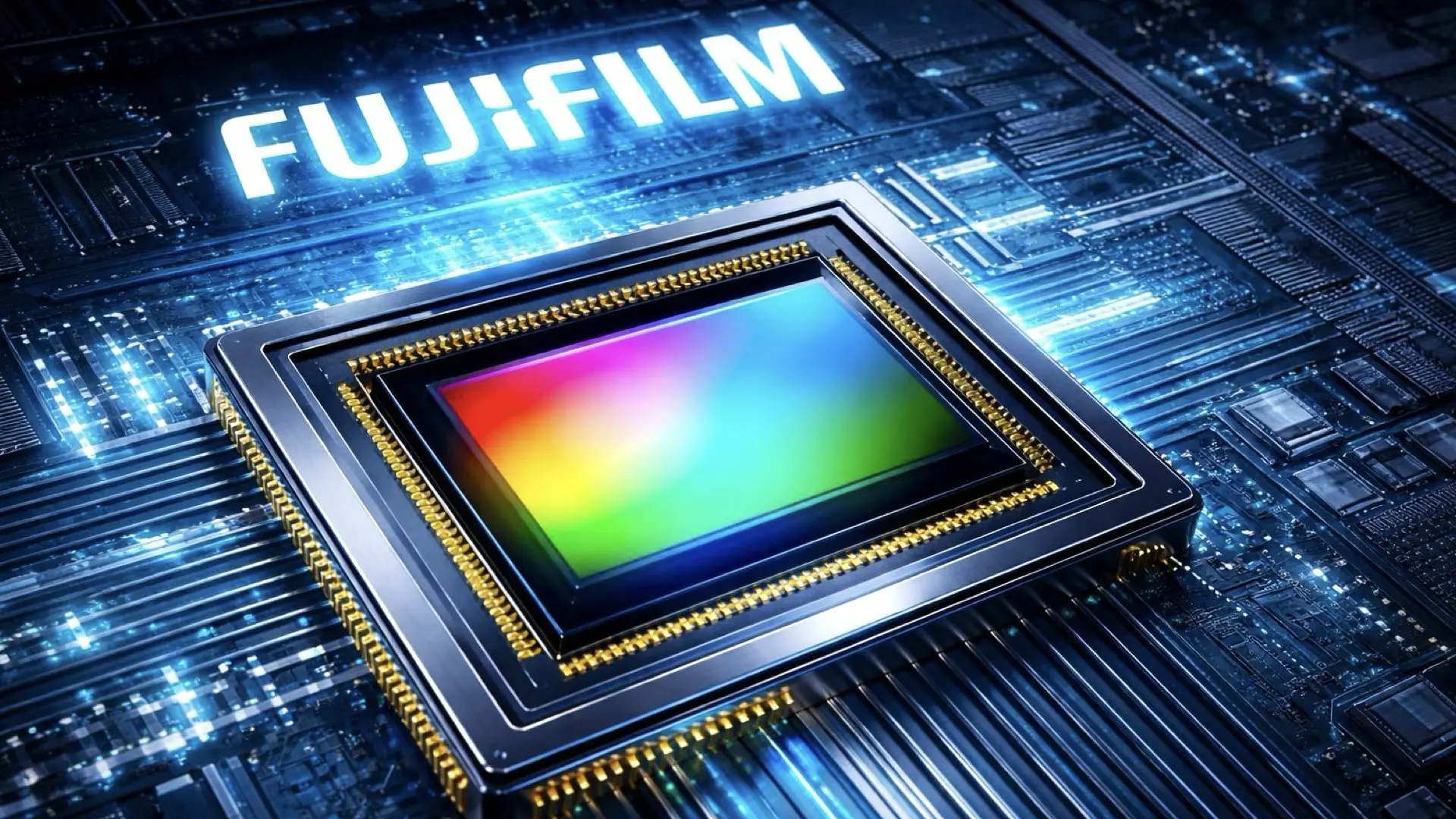
Fujifilm has announced a 5 billion yen investment in advanced semiconductor development. At first glance, this sounds distant from cinema cameras and image sensors. But for those who follow imaging technology closely, the move raises a deeper question. Is Fujifilm positioning itself closer to the future of sensor innovation?
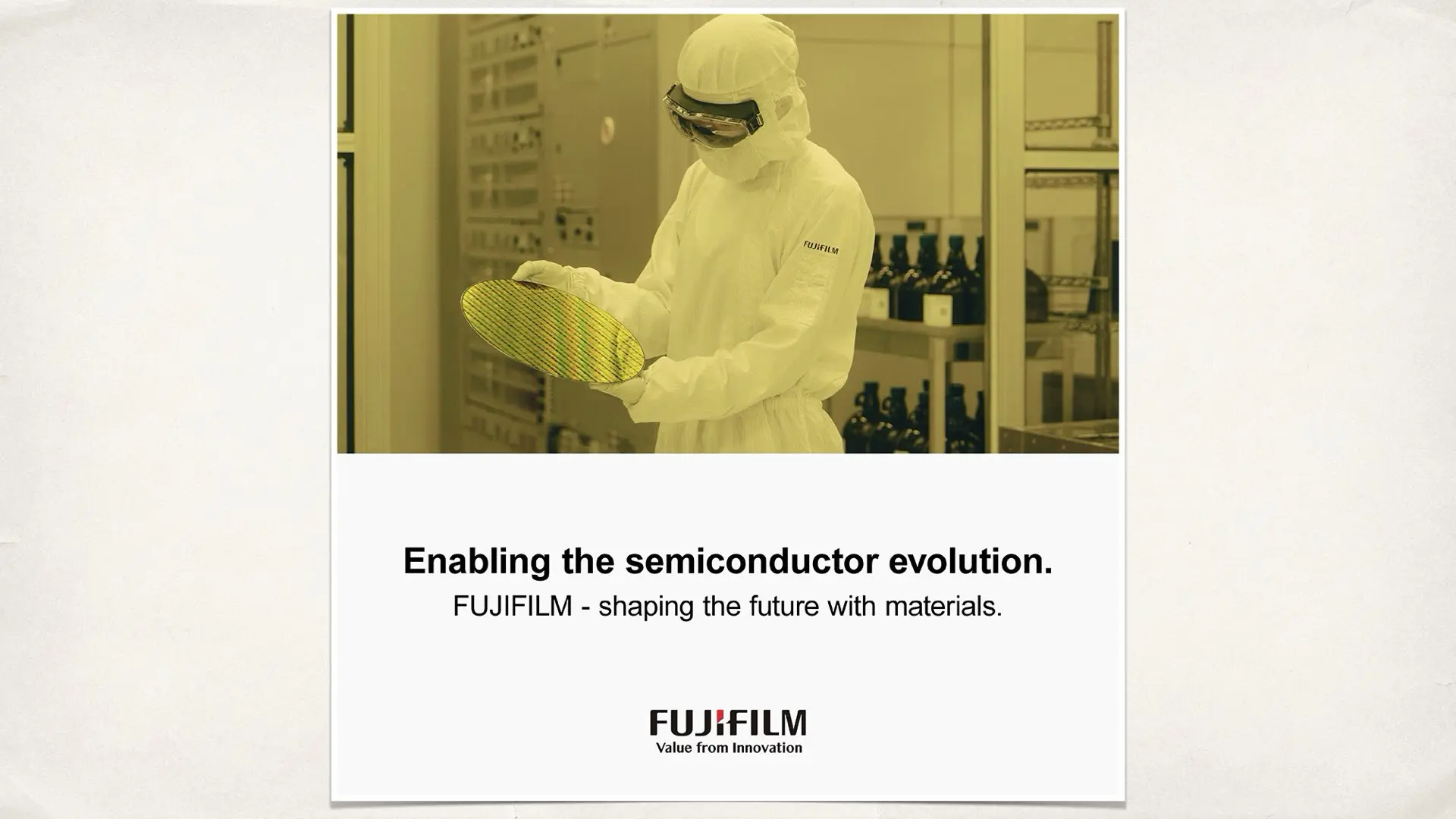
FUJIFILM Corporation announced that it has completed a 5 billion yen investment in Rapidus Corporation, a company aiming for the mass production of leading-edge logic semiconductors in Japan, following the execution of an investment agreement between the two companies. Through this investment, Fujifilm is committed to realizing the domestic mass production of leading-edge semiconductors and to the development of Japan’s semiconductor industry. As a semiconductor materials manufacturer, Fujifilm will strongly support Rapidus’ development and manufacturing of leading-edge semiconductors by providing a wide range of semiconductor materials and technologies. In addition, by working closely with Rapidus on next-generation process development, Fujifilm will enhance its technological capabilities and accelerate the development of materials for next-generation semiconductors.
– FUJIFILM
Understanding Fujifilm’s real role in semiconductors
Fujifilm does not manufacture image sensors. It does not design stacked CMOS architectures, global shutter pixel structures, or high-speed readout circuits. Those areas remain dominated by companies such as Sony, Samsung, and a handful of specialized players. However, Fujifilm plays a critical upstream role. The company is one of the world’s major suppliers of semiconductor materials. These include advanced photoresists, polishing slurries, and ultra-high-purity process chemicals. Without these materials, leading-edge chips cannot be fabricated with precision. In other words, Fujifilm operates at the materials layer of the semiconductor ecosystem. That layer rarely makes headlines in the imaging press, yet it sits beneath every sensor wafer produced anywhere in the world.

Why semiconductor materials influence image sensors
Modern image sensors are no longer simple photodiode arrays. High-end sensors used in cinema cameras increasingly rely on stacked architectures, where a light-sensitive layer is bonded to a logic layer underneath. That logic layer can include memory, signal processing blocks, and increasingly complex readout circuits. As pixel sizes shrink and processing density increases, fabrication tolerances become tighter. Advanced lithography and process control are essential. The chemistry and materials used during wafer processing directly influence yield, uniformity, and electrical performance. When Fujifilm strengthens its position in advanced semiconductor materials, it strengthens its visibility into the manufacturing frontier. That frontier includes the processes that enable faster readout speeds, lower noise floors, and higher dynamic range in future sensors. This does not mean Fujifilm will suddenly design its own image sensors. But it does mean the company deepens its integration with the technological layer that shapes what sensors can become.

A strategic rather than immediate shift
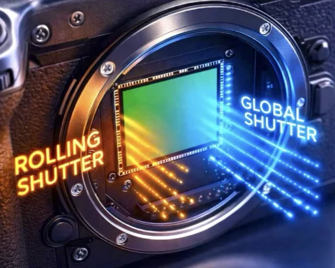
It is important to remain precise. This investment does not transform Fujifilm into a sensor powerhouse overnight. It does not give Fujifilm intellectual property in stacked sensor design. It does not give it control over sensor fabrication lines. What it does is reinforce Fujifilm’s role in next-generation semiconductor process development. That gives the company earlier exposure to new lithography challenges, scaling limits, and material constraints. For imaging technology, those constraints often determine the ceiling of innovation. Rolling shutter artifacts are influenced by readout architecture. Global shutter performance depends on pixel design and charge handling. On sensor processing for AI autofocus relies on dense, efficient logic layers. All of those features sit on top of semiconductor process capabilities. By aligning itself more deeply with advanced chip manufacturing, Fujifilm places itself closer to the technological conversations that define those capabilities.

The imaging ecosystem perspective
Our readers understand that camera innovation rarely happens in isolation. Sensor performance improvements often trace back to breakthroughs in semiconductor engineering. The rise of backside illumination, stacked CMOS, and high-speed readout layers followed advances in wafer bonding and fine patterning. Companies that supply materials to this ecosystem operate in the background, but they are part of the same value chain. If Fujifilm enhances its technological expertise through collaboration at the leading edge of chip fabrication, that expertise can feed back into its broader imaging and electronics businesses. The company already operates across medical imaging, industrial systems, and photographic technologies. Strengthening semiconductor capabilities reinforces that entire portfolio. From an ecosystem perspective, this move signals that Fujifilm wants deeper involvement in the technological foundations of imaging, even if it remains outside the direct sensor manufacturing arena. In cinema cameras, these advances translate into tangible features. Faster readout reduces rolling shutter distortion. Improved logic integration enables more sophisticated autofocus systems. Better process control can reduce noise and increase consistency across large sensors. Fujifilm’s strengthened position in semiconductor materials does not guarantee any specific sensor breakthrough. However, it increases the company’s proximity to the technical inflection points that shape sensor evolution. For a brand historically associated with film, color science, and medium format cameras, this reflects a broader transformation. Fujifilm has steadily diversified into high-value technology sectors. Deepening semiconductor involvement aligns with that trajectory.
What this does not mean
It is equally important to avoid overstating the case. Fujifilm is not entering direct competition with Sony in image sensor fabrication. It is not launching a new CMOS sensor line. It is not announcing a proprietary stacked sensor architecture. The power structure of the image sensor market remains largely unchanged. Dedicated sensor manufacturers still control design, production, and intellectual property in that space. This development should be viewed as strategic positioning within the semiconductor materials domain, not as a declaration of sensor dominance. When analyzing industry shifts, the most interesting movements often happen beneath the product layer. Cameras evolve every year, but the foundational technologies enabling those cameras evolve over decades. Fujifilm’s 5 billion yen investment signals confidence in advanced semiconductor development. It reinforces the company’s ambition to remain technologically relevant in high-precision manufacturing fields. For filmmakers and imaging professionals, this does not change the camera lineup tomorrow. It does suggest that Fujifilm is strengthening its technological backbone in areas that underpin future sensor capabilities. Whether that translates into tangible advantages for Fujifilm-branded cameras remains to be seen. What is clear is that the company is deepening its engagement with the semiconductor layer that defines modern imaging. The question then becomes less about immediate impact and more about the course. By embedding itself further into advanced semiconductor development, Fujifilm positions itself closer to the technological currents that will shape the next generation of image sensors.


Doesn’t Fujifilm develop its own line of X-Trans sensors.
x-trans is just another colour-filter arrangement. All so-called “x-trans sensors” are basically just standard Sony IMX-series sensors with customised CFAs.