Onsemi and ARRI have long term relationship and partnership regarding the outstanding ALEV sensors. A few days ago, Onsemi (aka ON-Semiconductor) was awarded an Emmy for Technology and Engineering by the National Academy of Television Arts and Sciences (NATAS) for engineering creativity, regarding its intra-pixel charge transfer CMOS image sensors. Onsemi chose to thank ARRI for utilizing Onsemi sensors to enable “Best-in-class image capture” by ARRI cameras.

Onsemi + ARRI = ALEV Sensors
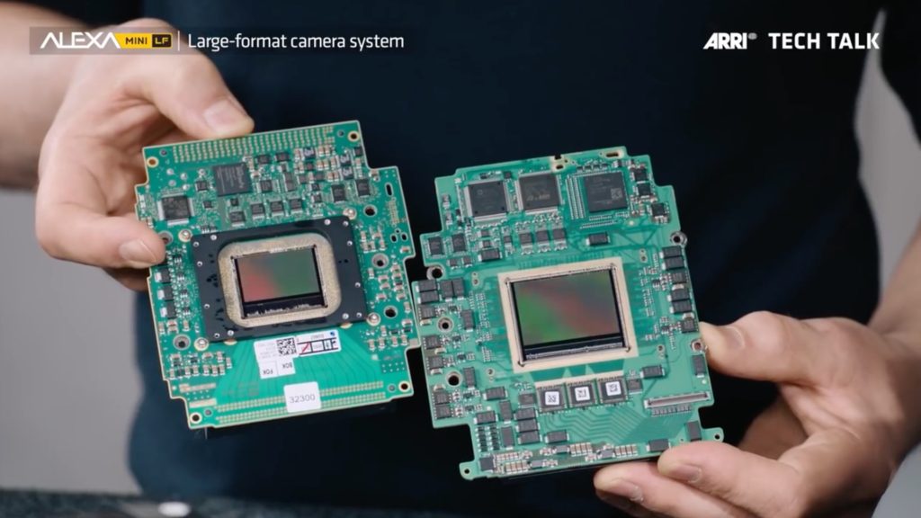
ARRI cameras utilize the CMOS sensors invented by ON Semiconductor (Onsemi). These are custom-developed ALEV III CMOS Bayer sensors used in the ALEXA and AMIRA series of cameras. Onsemi has just received the Emmy Award for Technology and Engineering from the National Academy of Television Arts and Sciences (NATAS). Industry experts and peers chose the company’s work in the pioneering design and development of its intra-pixel charge transfer CMOS image sensors for showing excellence in engineering creativity. This is the 3rd time that ON accepts the Emmy Technology & Engineering Award. As ARRI stated before: “Our success with ALEXA reflects directly on the strong partnership we continue to enjoy with ON Semiconductor for this critical imaging component”.
By utilizing our technology, we have successfully delivered remarkable products that combine exquisite image quality at high resolution and frame rate to enable best-in-class image capture.
Ross Jatou, senior vice president, intelligent sensing group at Onsemi
More than 20 years of partnership
As stated by Onsemi: “For more than 20 years, Onsemi has worked with ARRI, a leading manufacturer of motion picture equipment in the world, to bring high-quality digital capture to professional motion picture and television production. Camera-specific adjustments by ARRI combined with the advanced image sensors from Onsemi allow capturing the color richness, vibrancy, and high dynamic range that previously cinematographers depended on film to deliver. By working in a digital medium, cinematographers get the benefits of fully digital workflows for editing and post-production effects”. Ross Jatou, senior vice president, intelligent sensing group at Onsemi said: “By utilizing our technology, we have successfully delivered remarkable products that combine exquisite image quality at high resolution and frame rate to enable best-in-class image capture.” Read the announcement here.
ALEV in ALEXA
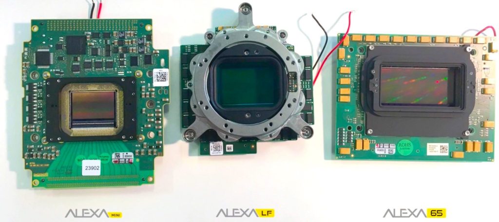
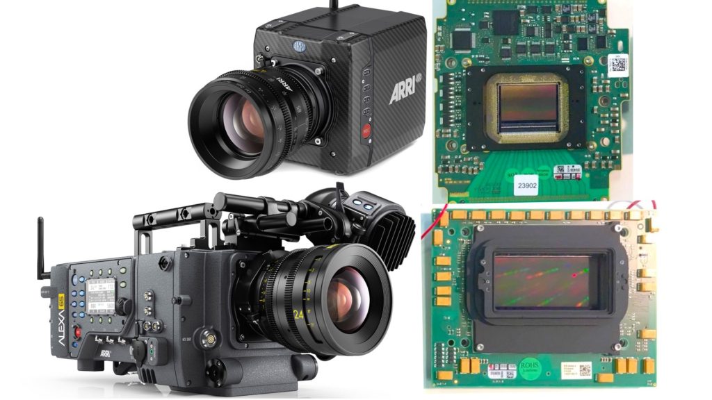
The ALEXA’s ALEV III image sensor has 3392×2200 effective pixels used for generating an image, 2880×2160 pixels are generally used for recording on the Alexa Studio and M in 4:3 mode, and 2880×1620 pixels are used for recording on the regular ALEXA and other models in 16:9 mode, the rest of the sensor is used for a look around in the viewfinder. Alternately the full sensor resolution may be employed in ‘Open Gate’ mode for a resolution demanding situations. The ALEXA 65 uses the A3X sensor, which has a 54.12 mm × 25.59 mm active imaging area. It provides up to 6560×3102 ‘Open Gate’ maximum recordable resolution. The ALEXA LF and ALEXA Mini LF use the A2X sensor, which has a 36.70mm × 25.54mm active imaging area. It provides up to 4448×3096 maximum recordable resolution.
What about the upcoming ALEXA 4K S35?
The forthcoming ARRI ALEXA 4K S35 camera will use the same ALEV III sensor as well. Why? Because never change a winning horse. This sensor will have almost the same dimensions as the ALEXA Mini Sensor.







Wait… isn’t the new camera using the brand new ALEV4 sensor? …this is why it has taken so long / the pixel size, etc is different? Been hearing about ALEV4 for a long time and never heard that it is also ALEV3… it’s brilliant but lord would it be disappointing if they continue to use the same sensor for 10+ years. I want to see how these companies can improve upon this brilliant sensor.
Yeah, this makes no sense. The photosites on the 4k s35 would have to be substantially smaller than Alev3 photosites. Plus just shrinking the size of photosites while using the same old tech would just reduce dynamic range.