Sony has published an article presenting its view and approach regarding stacked CMOS image sensors evolution. The article demonstrates Sony’s ambitions to further develop stacked sensors that will be capable of high-speed imaging, especially concerning large sensors. Explore the options and technologies below.
Evolving stacked sensor architecture
Here you can find this new article titled “Evolving Image Sensor Architecture through Stacking Devices” published by Yusuke Oike, which is a researcher and developer of CMOS image sensor architecture and device technology at Sony Semiconductor Solutions. The article demonstrates Sony’s approach to stacked technologies of image sensors of various needs. The chip size of image sensors varies depending on the optical size, ranging from 1/4 inch (3.6 mm x 2.7 mm) used in smartphones to 35 mm full-frame (36 mm x 24 mm) utilized in high-end consumer cameras. Furthermore, in between the lines, we can explore Sony’s view regarding high-speed imaging, which is achieved via different architectures. We’ve concluded the key points relevant to our industry (large sensor consumer cameras).

Stacked CMOS architecture: CoC vs. Wow
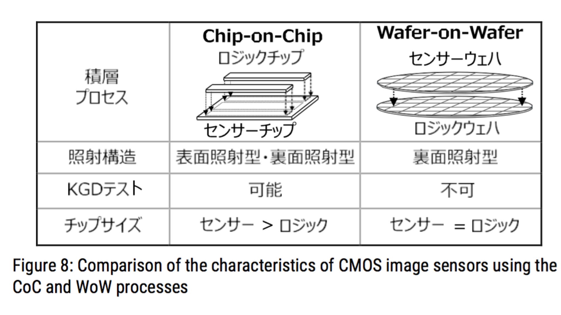
The slide below shows a comparison between the Chip-on-Chip (CoC) process, which stacks individual chips, and the Wafer-on-Wafer (WoW) process, which stacks wafers together. The mainstream stacked structures, mainly image sensors for smartphones, use the WoW process, which has the advantage of high yield, but the size of the sensor chip and the logic chip must be the same. On the other hand, the CoC stacked structure allows the individual logic chips to be attached to the sensor chip. In other words, the big difference is that there is no need to attach a large logic chip to an image sensor with large optical size. However, the CoC process offers a cost advantage over the WoW process when the peripheral circuit size is sufficiently small compared to the optical size.
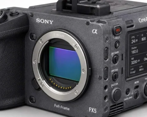
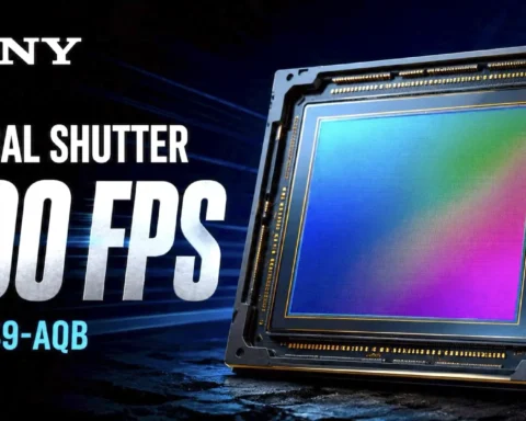
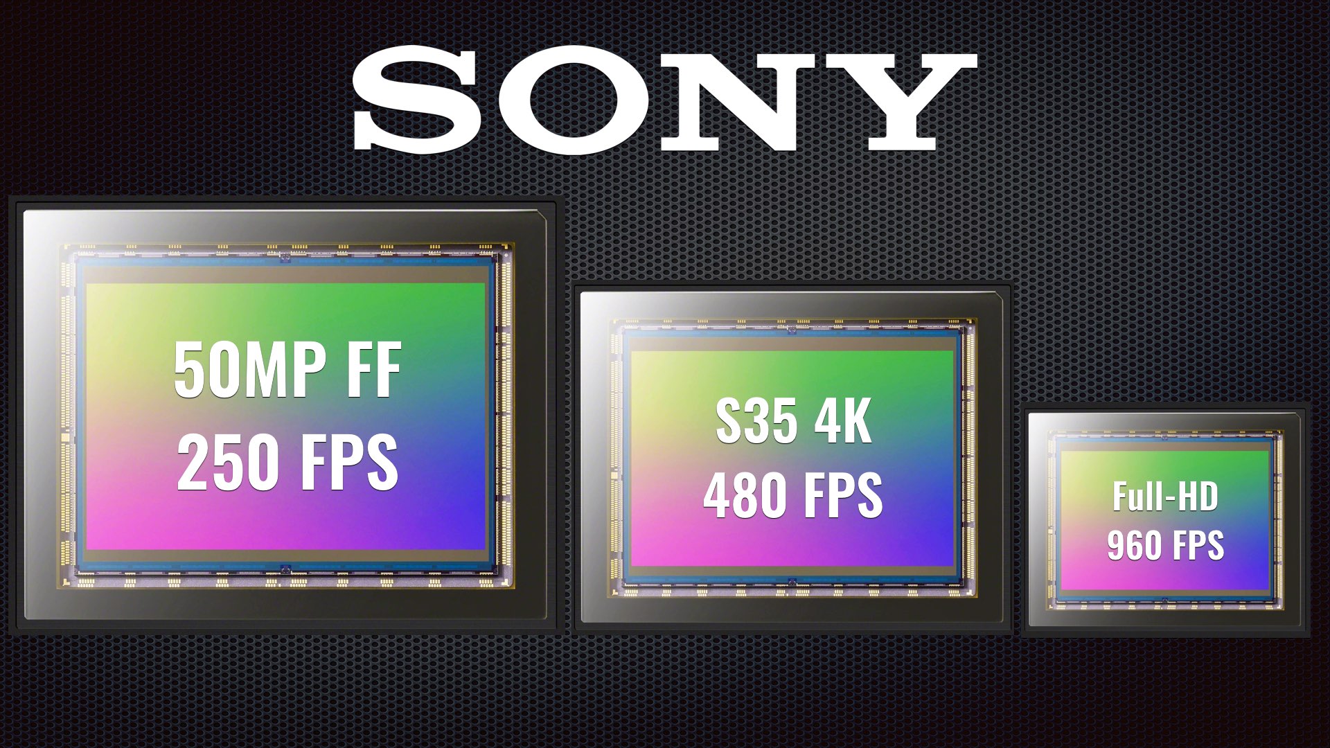
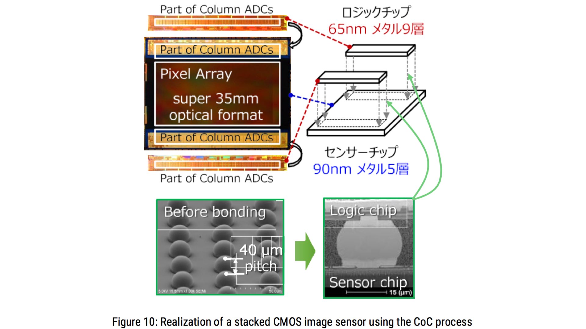
4K & 480 FPS in Super 35 global shutter
A stacked CMOS image sensor using the CoC process is shown in the scheme below. The optical size is Super 35 mm format (24 mm x 18 mm). At the time, the global shutter function, which enables distortion-free imaging of moving subjects, was available only in front-illuminated types. The CoC process is used to combine the global shutter function with the slow-motion shooting function at 4K resolution in a high-end professional broadcast camera, enabling video recording at 480 frames per second at 4K resolution of 8 megapixels. The current CoC process is not as productive as the WoW process, but as image sensors become more sophisticated and processors and memories based on advanced CMOS processes are required, the importance of the CoC process, which has a high degree of freedom in selecting the process for each function, may increase.
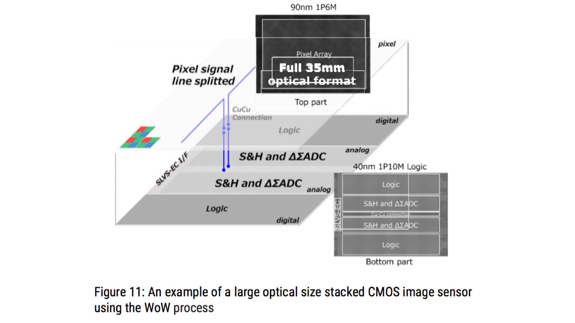
50MP full-frame sensor – 250 FPS
The sensor discussed is a full-frame, 50MP 250 FPS (most probably the sensor in the Alpha 1). The slide below shows an example of a modern 35 mm full-frame (36 mm x 24 mm) stacked CMOS image sensor using the WoW process. As mentioned earlier, the WoW process is suitable when the peripheral circuit size matches the optical size. A high frame rate of 250 frames per second at 50 megapixels is achieved by using multiple parallel ΔΣ ADCs that can operate at high speed with low noise for high-end single-lens cameras.
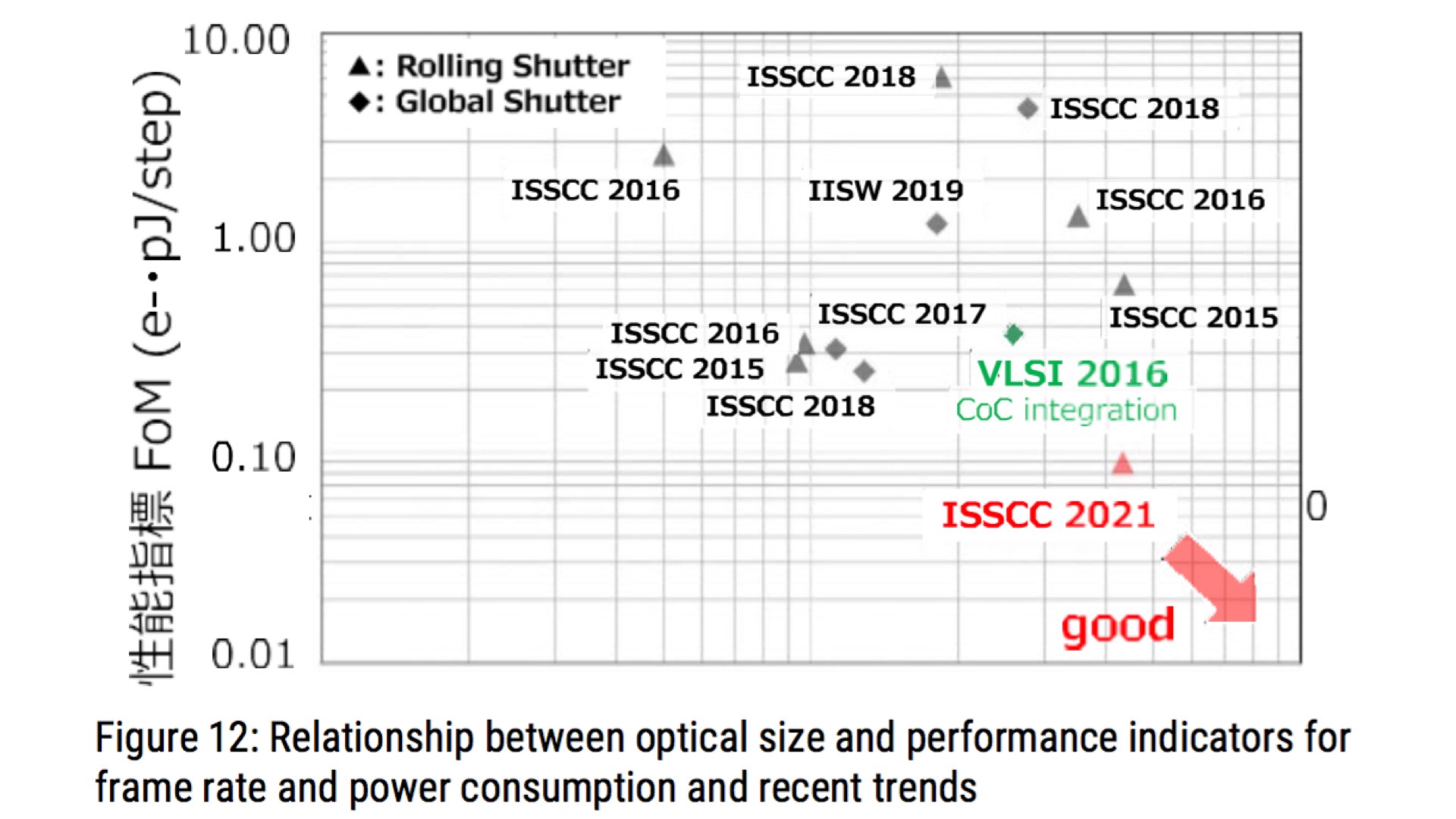
Another slide demonstrates the evolution of FoM (Figure of Merit), which is a performance index of electronic equivalent noise and energy consumption per AD conversion step, against optical size. Even in the case of large-format image sensors, where high speed is difficult to achieve, the use of a stacked structure has led to continued progress in achieving both high speed and high image quality.
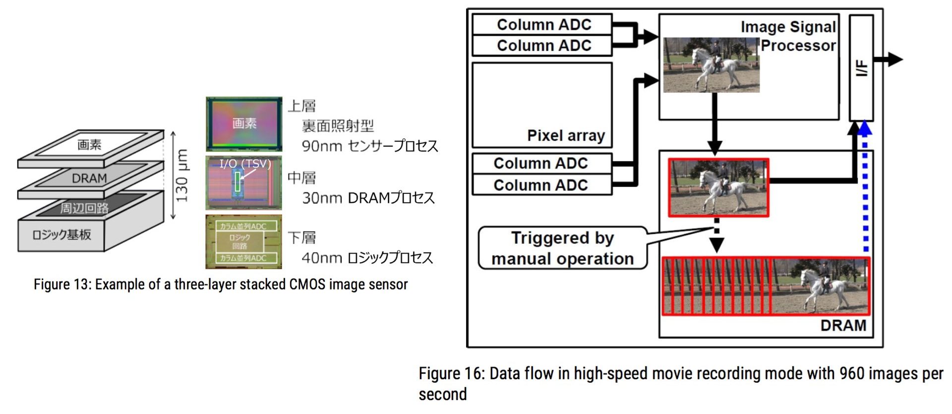
960 FPS in full-HD
By stacking the DRAMs directly on the image sensor, a 200 MHz 512-bit bus can be used to connect the DRAMs to the image processor. The DRAM is stacked directly on the image sensor to provide a low-power, 102 Gbps bandwidth link between the DRAM and the image processor. Using the DRAM buffer, Sony achieved a maximum of 960 frames per second at Full HD (1920 × 1080 pixels) resolution, as shown in slide 10. By temporarily buffering the data before and after a slow-motion scene in DRAM, Sony captures up to 960 frames per second at Full HD (1920 × 1080 pixels) resolution. Explore the following schema demonstration of the DRAM in stacked architecture.
Discussion
Sony utilizes stacked architecture in order to elevate FPS (Frame Per Second) on large sensors (above Super 35mm), focusing on prosumer cameras. Sony aims to improve both rolling and global shutters on CMOS, especially regarding FPS capabilities. As shown, Sony has managed to develop a 50MP full-frame sensor that is capable of 250 PFS and a high-speed global shutter stacked sensor. This article indicates Sony’s approach to utilizing DRAM in stacked architecture in order to increase FPS, and thus to reach ultra-high frame rates. These findings suggest a new generation of large-format image sensors that are capable of shooting ultra-high frame rates, combined with a very high pixel count, and without impairing the compact form factor of the cameras.
Product List
Here’re the products mentioned in the article, and the links to purchase them from authorized dealers.
- Sony Alpha 1 Mirrorless Digital Camera