

Future camera sensors may no longer function as passive imaging devices. A newly published Meta-backed research project introduces a radically different approach to image capture built around a 3-layer stacked computational sensor capable of approaching nearly 20 stops of dynamic range while integrating image processing directly inside the sensor itself. Although the prototype is tiny, the implications for the future of cinema cameras, computational photography, and AI imaging systems could be enormous. The paper, titled “A 400×400 3.24µm 117dB Dynamic Range 3 Layer Stacked Digital Pixel Sensor,” was presented at ISSCC 2025, one of the world’s most important semiconductor conferences. The research was developed by Brillnics in collaboration with Meta and reveals a future imaging direction where the line between image sensor and image processor begins to disappear.

A different kind of image sensor
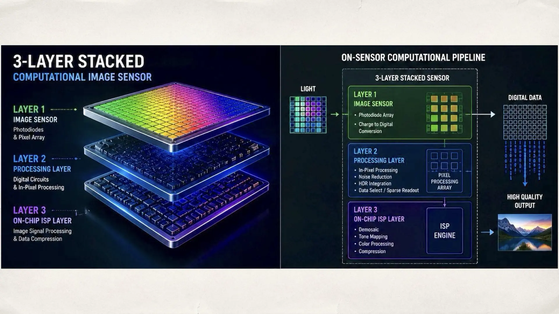
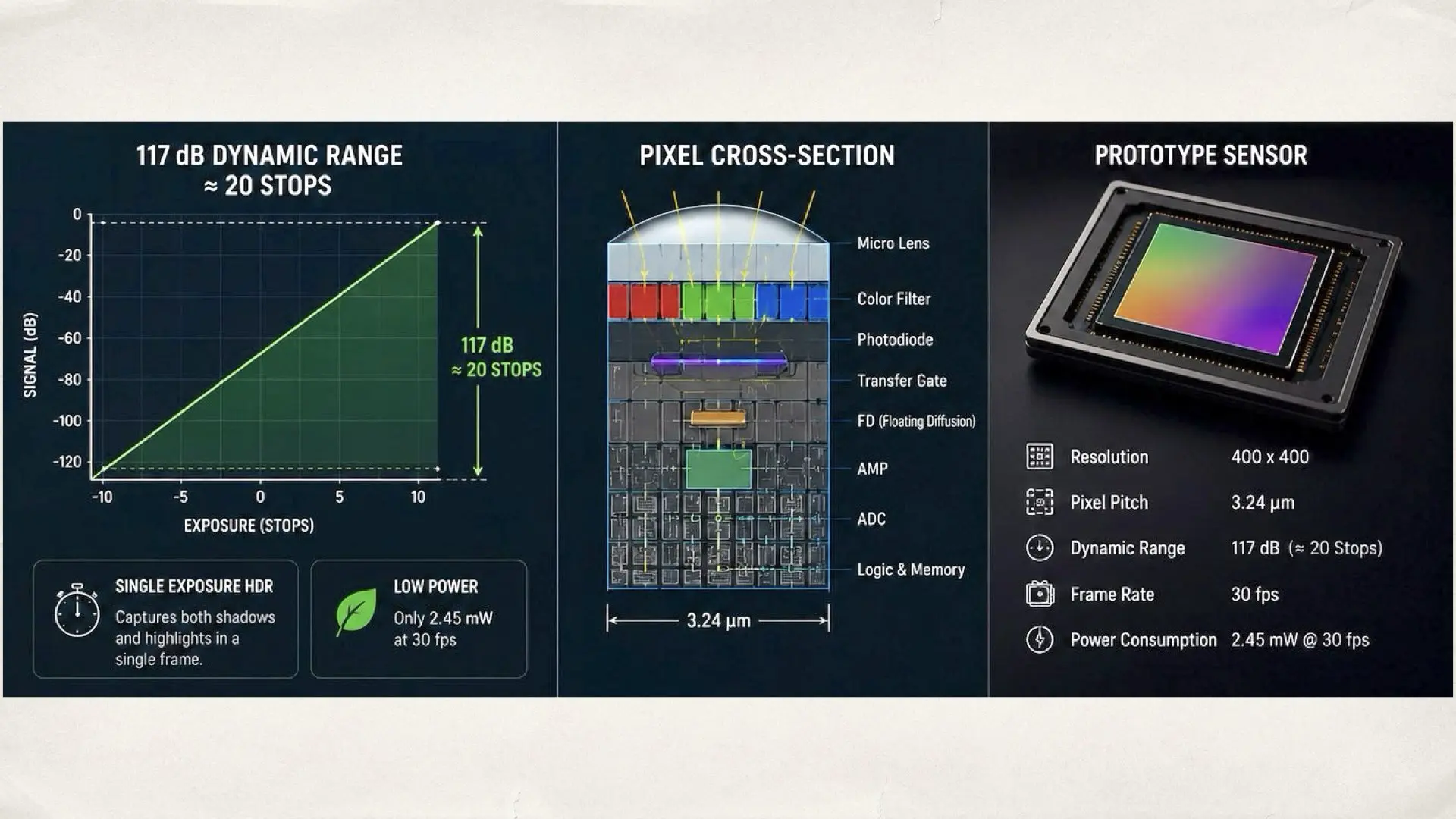
At first glance, the sensor itself may not appear especially impressive. The prototype resolution is only 400×400 pixels with a 3.24µm pixel pitch. However, the real breakthrough here is not the resolution. It is the architecture. The sensor combines a digital pixel sensor design with a 3-layer stacked structure and an integrated on-chip ISP. That means the sensor is no longer limited to simply capturing light. It is actively processing image data internally before the information even leaves the chip. This represents a major shift away from the traditional imaging pipeline used in modern cameras. Today’s systems typically operate like this: Sensor → ISP → CPU/GPU This research points toward a future where those boundaries become increasingly merged inside the sensor stack itself.
Why 117 dB dynamic range is such a big deal
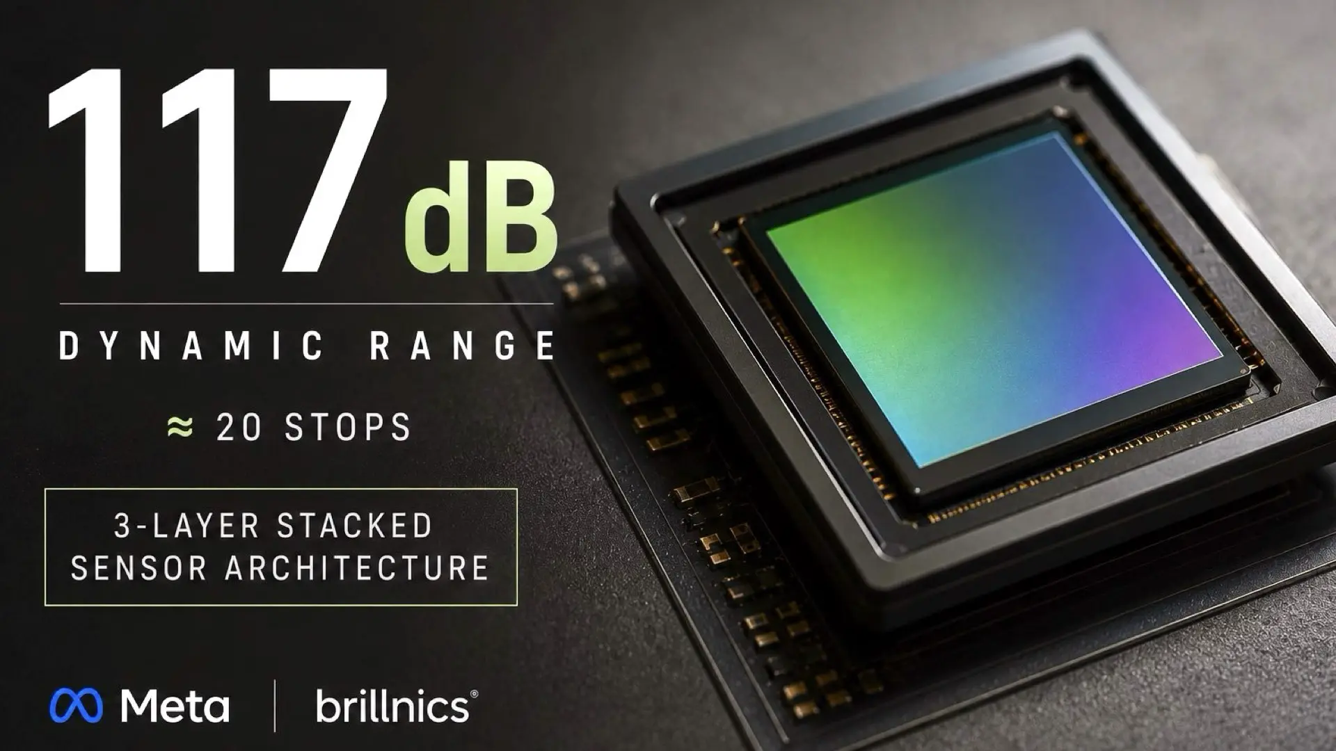
The most eye-catching specification in the paper is the claimed 117 dB dynamic range. Converted into photographic stops, that approaches roughly 19.4 stops of theoretical dynamic range. 1176.02≈19.4 stops. That number is enormous compared to most modern cinema cameras. However, the more important detail is how the sensor reportedly achieves this performance. According to the research, the architecture supports single exposure HDR capture rather than relying entirely on traditional multi-frame HDR merging. That distinction matters enormously for motion imaging. Multi-frame HDR systems often introduce ghosting, rolling inconsistencies, and motion artifacts during fast movement. Single-exposure HDR architectures are significantly more valuable for cinema and machine vision applications because they preserve temporal consistency across the frame.
The sensor itself is becoming the processor
One of the most important aspects of this research is the integrated on-chip ISP. For years, the imaging industry has gradually pushed toward computational photography and AI-assisted imaging. Smartphones already rely heavily on software processing pipelines, but this architecture moves computational functionality directly inside the sensor itself. The future direction appears increasingly clear. Tomorrow’s sensors may not simply capture photons. They may analyze, optimize, compress, tone map, and intelligently process visual information before the image even reaches the main processor. The paper also references sparse data transmission and pixel digital processing functionality, both strongly associated with future AI imaging systems and edge computing architectures. This direction could dramatically reduce bandwidth requirements, power consumption, latency, and thermal output.
Meta’s involvement
Meta’s involvement immediately expands the importance of this research beyond academic semiconductor engineering. The company continues investing heavily in AR glasses, spatial computing, wearable AI systems, and always-on machine vision technologies. Those future devices will require imaging systems capable of delivering high dynamic range, low power consumption, compact size, and integrated computational processing simultaneously. This sensor appears perfectly aligned with that future. The reported power consumption is especially impressive. The entire system reportedly consumes only 2.45 mW at 30 fps, an extremely low figure for a sensor architecture capable of 117 dB dynamic range. That level of efficiency strongly suggests wearable and edge AI applications rather than conventional camera products alone.
For the future of cinema cameras?
The tiny 400×400 resolution may initially make the sensor seem unimportant for professional imaging applications. In reality, many breakthrough sensor technologies first appeared in small experimental arrays before eventually scaling into larger commercial systems. Backside illuminated sensors, stacked DRAM architectures, advanced HDR systems, and global shutter technologies all followed similar developmental paths. The purpose of this prototype is clearly to validate the architecture itself rather than compete with commercial camera sensors. The important question is not whether this exact sensor will appear inside a cinema camera. The real question is whether the underlying architecture can eventually scale into larger imaging systems. Although this research is likely aimed primarily at AR, AI, and machine vision systems, the implications for cinema technology are fascinating. Future cinema sensors may eventually integrate: real-time HDR processing, computational tone mapping, AI-assisted noise reduction, advanced motion analysis, and low-latency image optimization directly inside the sensor stack itself. That does not mean large sensor physics suddenly becomes irrelevant. Sensor size still plays a massive role in light gathering, noise performance, depth rendition, and cinematic rendering characteristics. However, the future of imaging increasingly appears computational as much as optical. Sony, Canon, and Samsung have already pushed aggressively toward stacked sensor architectures. This Meta-backed research suggests the next major frontier may involve sensors that function as intelligent imaging systems rather than passive light capture devices. Our two cents that in the future, the camera sensor may no longer be just a sensor. It may become the heart of the entire imaging pipeline. Source: A 400×400 3.24-μm 117-dB Dynamic Range Three-Layer Stacked Digital Pixel Sensor With Triple Quantization and Fixed Pattern Noise Correction


There’s something wrong with your math here. 117 dB is approximately 38.9 stops, not 20. Each stop is a doubling or halving of irradiance, not field strength.