
Canon has introduced a new lithography system with a large exposure field at a high resolution for producing full-frame CMOS sensors, XR devices, and others. The machine titled FPA-5550iX is a significant step for Canon to strengthen its position as a full-frame sensor manufacturer.
Manufacturing sensors by lithography systems
A lithography system is a crucial piece of equipment used to manufacture semiconductor chips. The most important step in semiconductor device fabrication is lithography where a circuit pattern is transferred from a mask to a wafer or panel by precision Semiconductor Lithography Equipment commonly referred to as steppers or scanners. Canon has developed a lineup of Semiconductor Lithography Equipment designed to meet the technical requirements of a wide range of applications in addition to traditional semiconductor wafer processing.
Overview of Semiconductor Lithography Equipment
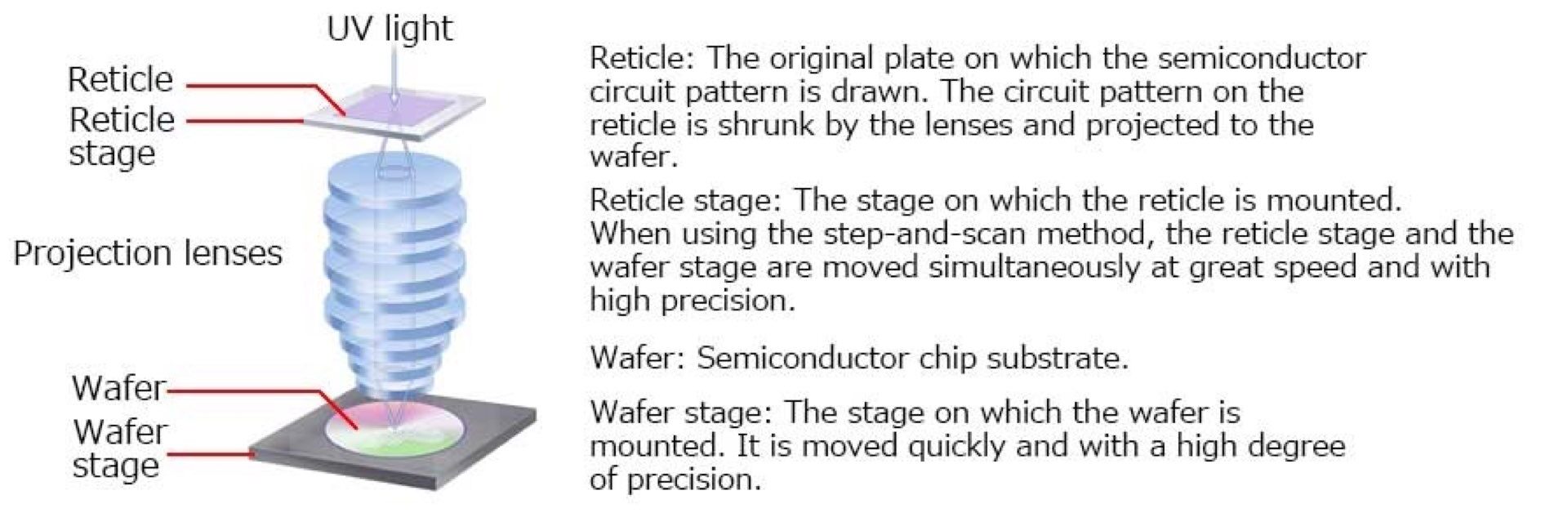
Semiconductor lithography equipment is used to perform exposure, part of the semiconductor chip manufacturing process. Semiconductor chips are created by performing exposure of microscopic circuit patterns on semiconductor substrates called “wafers.” Semiconductor lithography equipment exposes wafers by using projection lenses to reduce the circuit pattern of an original plate, called a “reticle.” This equipment consists of three mechanisms: a reticle stage, a projection optical system comprising multiple lens groups, and a wafer stage. The reticle on which the electronic circuit pattern has been drawn is placed on the reticle stage. Ultraviolet (UV) light is then shined down through it from above. The UV light that passes through the reticle is relayed through the projection optical system, forming an image of the reticle’s electronic circuit pattern on the semiconductor substrate placed on the wafer stage. A resin, called “resist,” has been applied to the surface of the wafer in advance. This resist undergoes changes when it is exposed to UV light, so the electronic circuit pattern on the reticle is transferred to the areas on which the UV light shines. The semiconductor chip manufacturing process can be broadly divided into three processes:
- The design process, in which the wiring circuits are designed
- The front-end process, in which electronic circuit patterns such as transistors and wiring are transferred to a semiconductor wafer through exposure
- The back-end process, in which wafers with electronic circuits formed on them are divided into individual chips and assembled
A major step for FF sensors
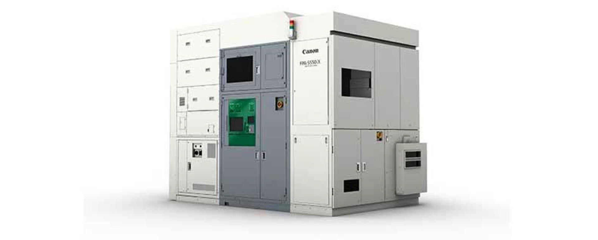
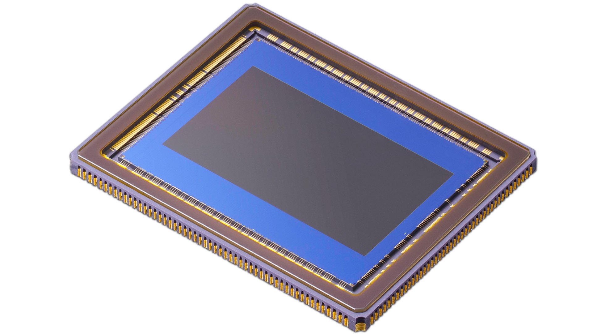
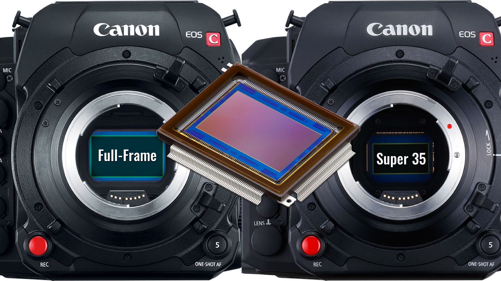
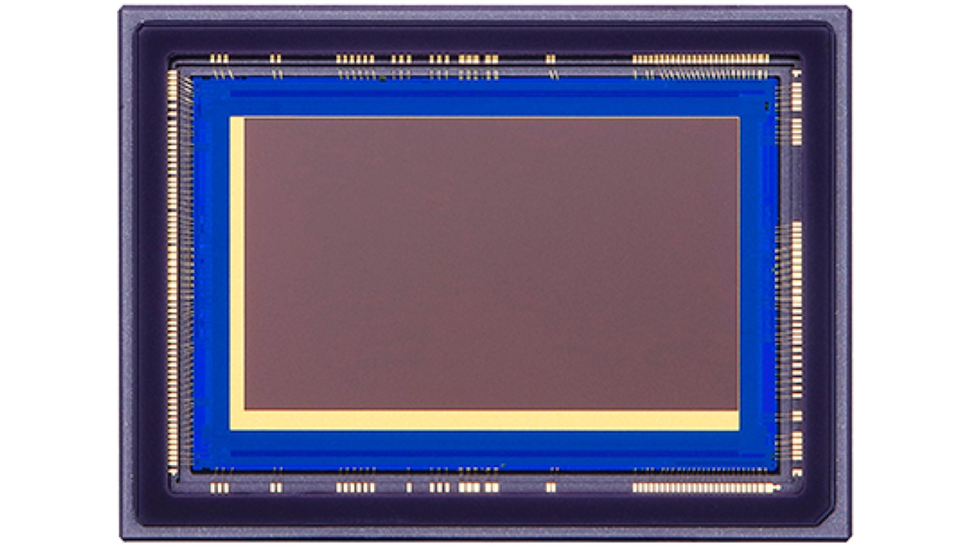
Now let’s get to the news. Canon has announced that the company will release the FPA-5550iX i-line stepper semiconductor lithography system for front-end processes that realizes a large exposure field of 50 x 50 mm and a high resolution of 0.5 micrometers. The new system features a large exposure field of 50 x 50 mm and a high resolution of 0.5 micrometers making possible single exposure of a large field with the high resolution required to produce full-frame CMOS sensors and other devices in which higher precision is advancing.
Not just for image sensors
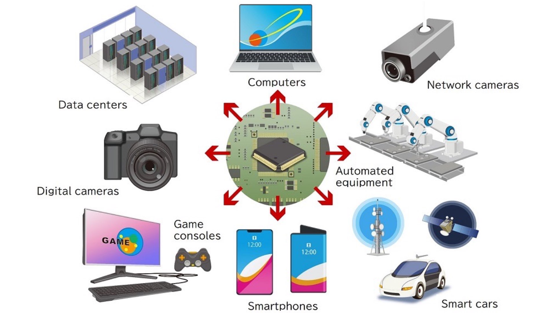
The new system is also capable of manufacturing small displays for such devices as head-mounted displays. It also enables the high-resolution single exposure required for manufacturing high-contrast micro-OLED panels with wide viewing angles, which are expected to grow as displays for cutting-edge XR devices. In addition to semiconductor devices, the new FPA-5550iX can also manufacture displays for cutting-edge XR devices, thus supporting the manufacture of a wide range of devices.
Dedicated to full-frame sensors
The FPA-5550iX utilizes the same projection lens used by its predecessor model, the FPA-5510iX (released in September 2015) which enables a high resolution of 0.5µm. Thanks to a wide exposure field of 50 x 50 mm, the system can perform high-resolution single exposure for full-frame CMOS sensors, next-generation displays for XR devices, and more. What’s more, manufacturing processes have been refined to ensure high-quality, stable production of projection lenses, many of which are used in the system, to meet the strong demand expected for semiconductor lithography systems. Furthermore, the system can optionally select an infrared wavelength that can pass through silicon, enabling users to measure the alignment on the back of the wafer, which is a requirement for the manufacture of back-illuminated sensors. The flexibility of alignment mark measurement thus allows the system to be utilized in a variety of processes.
Wrapping up
It is well known that Canon has the rare ability to produce its own sensors, including ultra-high-resolution large-format image sensors. However, the FPA-5550iX strengthens Canon’s capabilities to focus even more on full-frame sensors, especially the advanced back-illuminated sensors. Of course, those advanced CMOS image sensors can be implemented on Canon’s high-end cameras.
Support Y.M.Cinema Magazine by purchasing our one-of-a-kind stainless steel model of 65 motion picture film camera – A perfect gift for filmmakers.