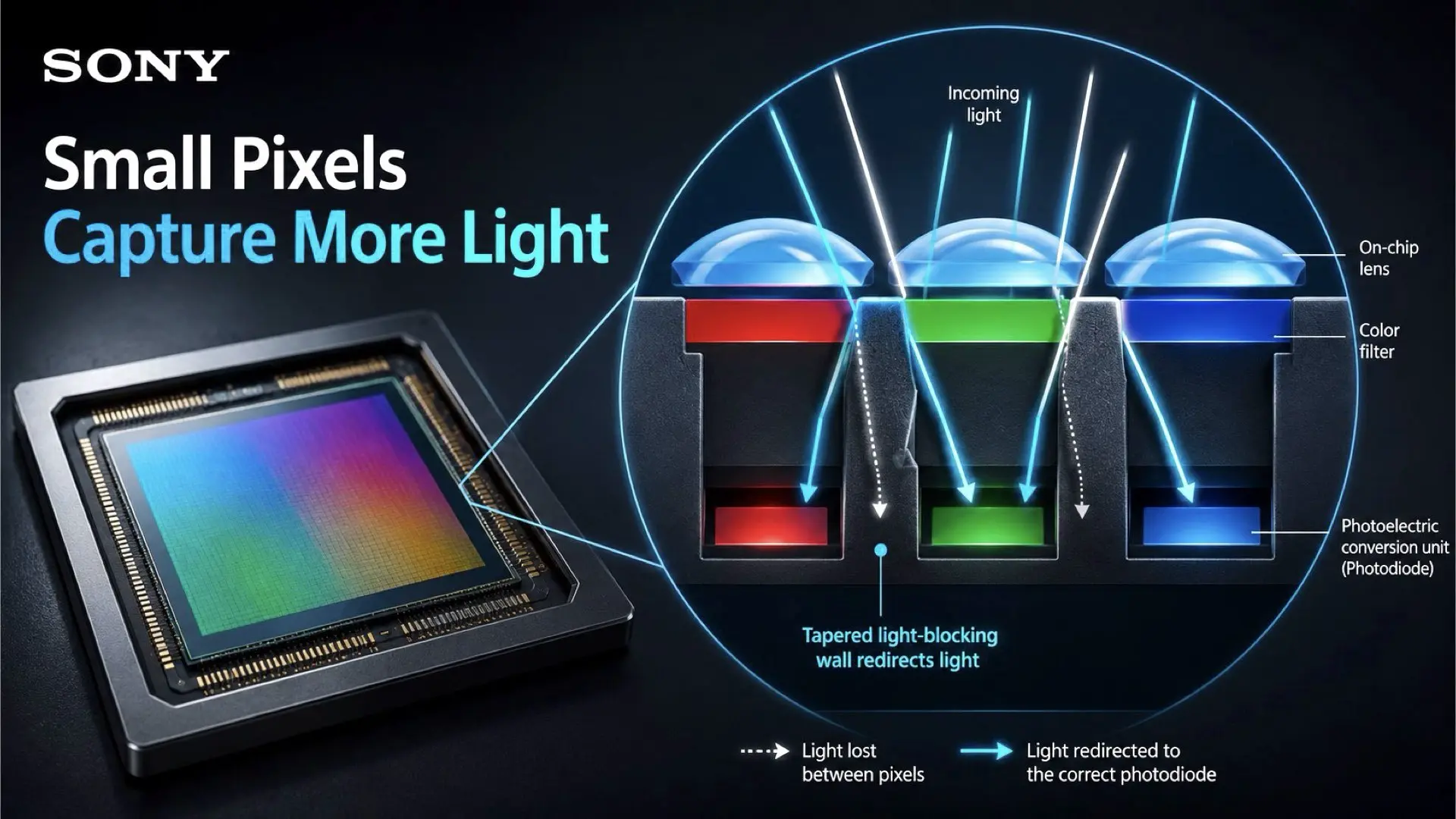
Sony is trying to develop an image-sensor design aimed at improving sensitivity by recovering light that would normally be lost between pixels. While the patent does not specify a particular sensor size or product, the concept appears especially relevant to small, high-resolution sensors such as those used in smartphones. The idea is surprisingly simple. Every image sensor is made from millions of individual pixels. Each pixel includes a photodiode that converts incoming light into an electrical signal. Above it sits a tiny on-chip lens that helps direct light toward the photodiode. The problem is that not every photon lands exactly where it should. Some light reaches the boundaries between pixels, where structures are required to separate one pixel from another. Instead of reaching the photodiode, some of this light can be absorbed, reflected inefficiently, or even enter a neighboring pixel. Sony’s patent proposes changing those pixel boundaries.
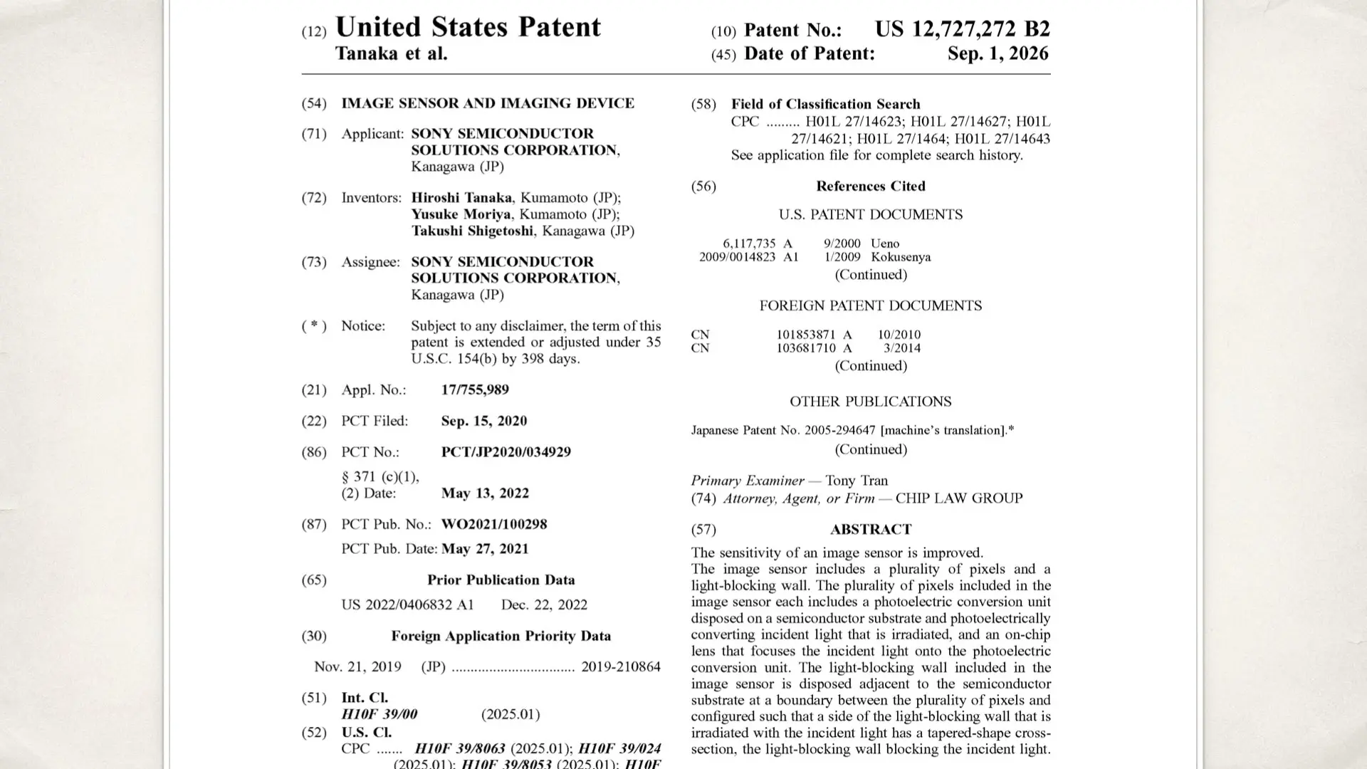
Turning pixel walls into tiny reflectors
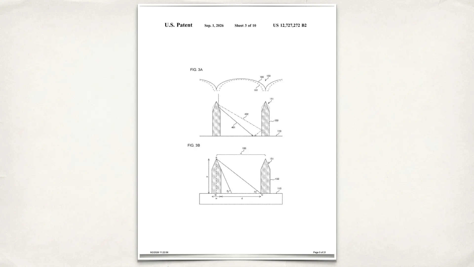
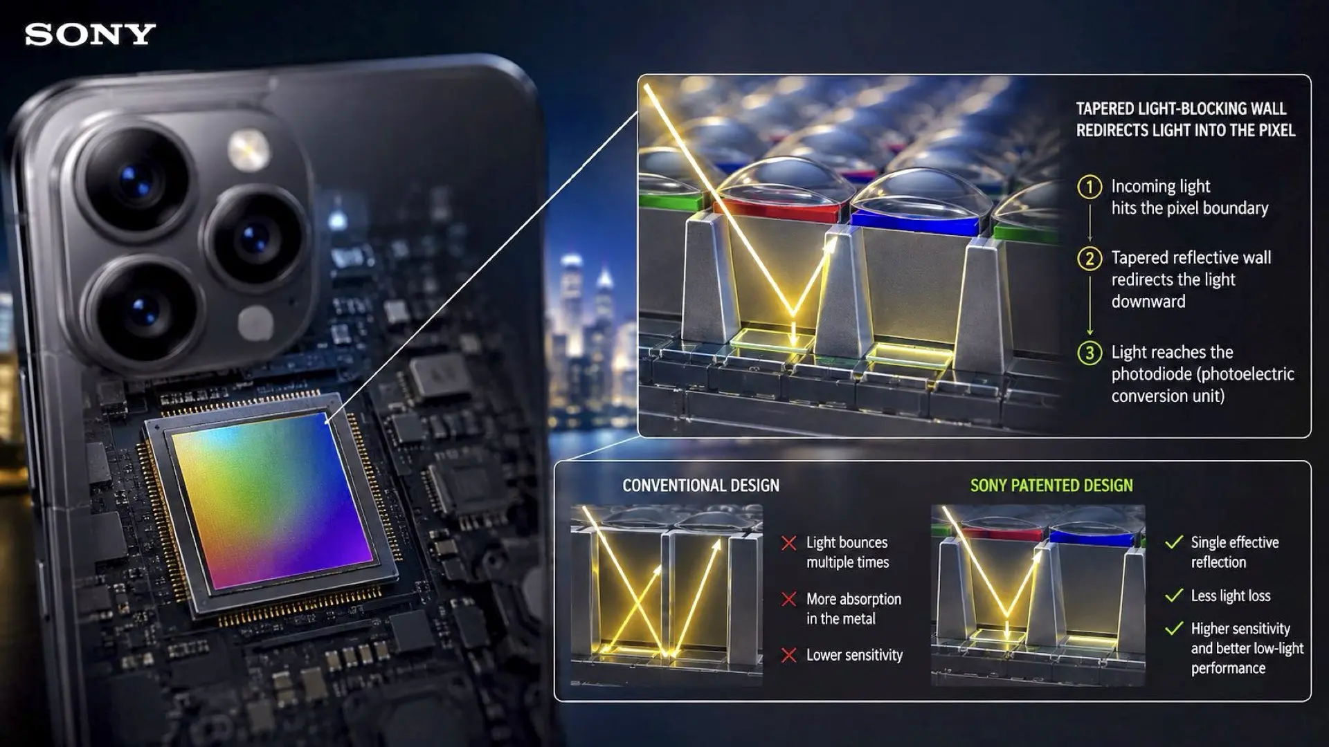
The design uses what Sony calls a light-blocking wall between adjacent pixels. The wall can be made from reflective metal and surrounds the light-sensitive area of each pixel. The important part is its shape. Instead of having a flat top, Sony proposes giving the wall a tapered, angled surface. Light hitting this area can then be reflected downward toward the photodiode rather than being wasted. Sony describes the goal as directing the light toward the semiconductor substrate after essentially a single useful reflection. Multiple reflections are less desirable because metallic surfaces are not perfectly reflective. Every additional bounce can absorb some of the incoming light. In other words, Sony is trying to collect light that the sensor already receives but does not normally use efficiently.
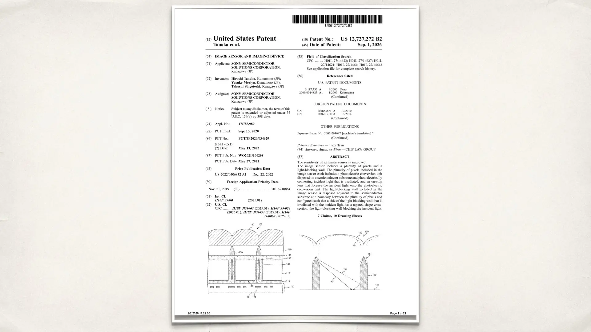
Why this is relevant for small pixels
This becomes particularly interesting as pixels get smaller. High-resolution sensors need to fit more pixels into the same physical area. Smartphone cameras are perhaps the most obvious example, with manufacturers routinely using sensors containing tens or even hundreds of millions of very small pixels. As pixel dimensions decrease, the physical structures surrounding each pixel become increasingly important. Losing even a small amount of light around the edges can hurt sensitivity. Sony’s approach could reduce some of that loss. The patent even gives an example involving a light-receiving area approximately 1.5 micrometers wide, together with nanoscale structures around the pixel. Sony does not state that this represents a commercial sensor or an actual future pixel pitch, but the dimensions illustrate the scale at which the technology can operate. That makes smartphones and other compact imaging systems a logical potential application.
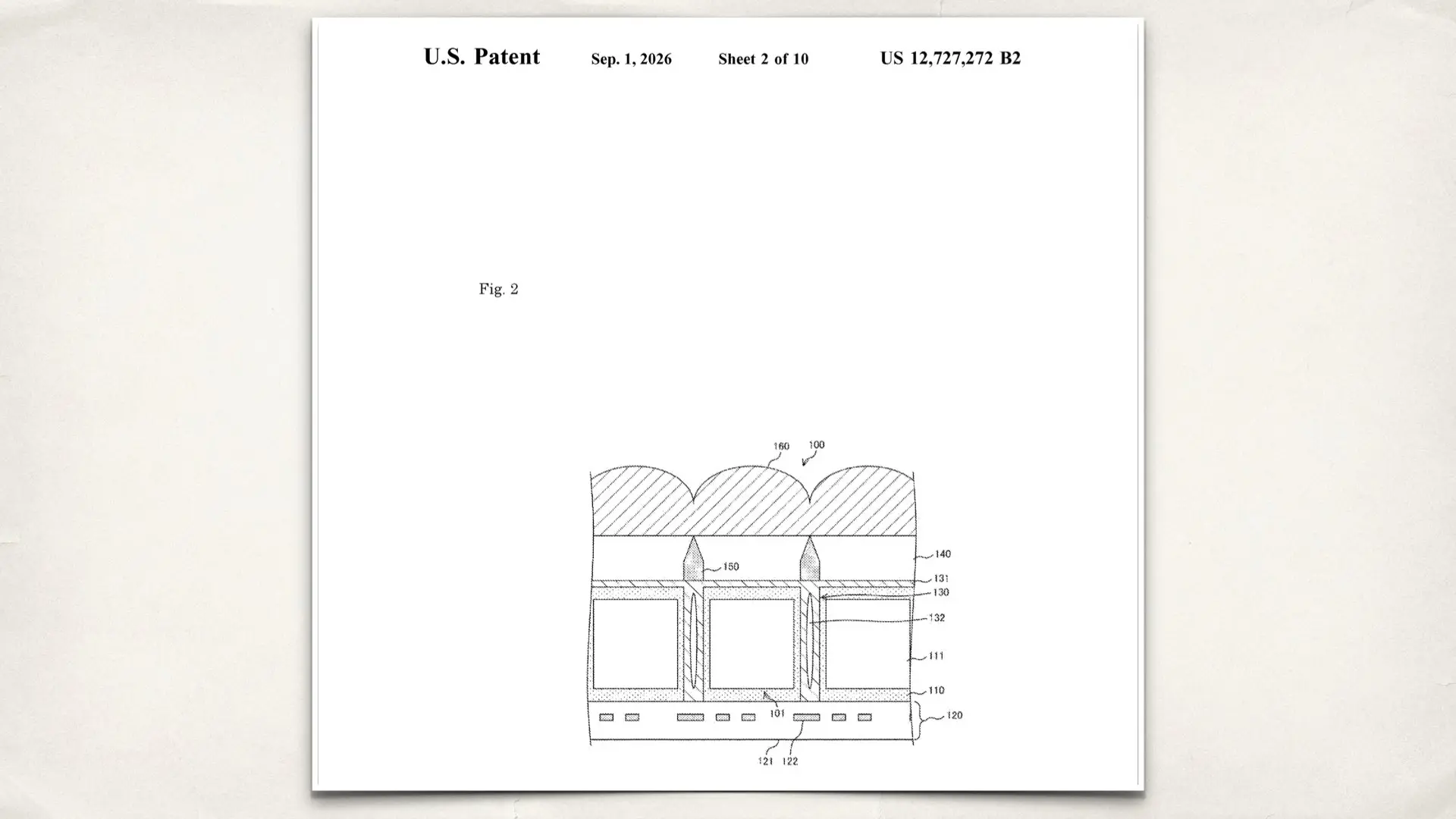
More sensitivity without simply making the pixel bigger
The interesting aspect of the patent is that Sony is not proposing a larger photodiode. Instead, it is trying to improve how efficiently light reaches the existing photodiode. The light-blocking wall still helps prevent optical crosstalk, where light intended for one pixel enters another. But its tapered surface can also redirect some of the light hitting the boundary back toward the correct pixel. This could potentially improve signal-to-noise performance in low-light conditions, particularly for very small pixels. Sony itself describes the benefit primarily in terms of increased sensitivity and clearer images in low-light environments. Importantly, the patent does not provide dynamic-range measurements, sensor resolution, sensor size, readout speed, or specifications for a particular camera. It should therefore not be interpreted as a new Sony smartphone sensor announcement.
Not necessarily limited to smartphones
Although small sensors appear to be an obvious use case, the same principle could also become relevant to larger sensors as resolution increases. A very high-resolution APS-C or full-frame sensor can also contain relatively small pixels. Recovering light that would otherwise be lost between those pixels could therefore be useful there as well. The patent’s main implementation is described using a backside-illuminated sensor architecture, although Sony notes that the concept can also be used with frontside-illuminated sensors. Ultimately, the patent represents another way of improving image sensors without simply increasing their physical size. As camera sensors continue packing more pixels into limited space, making better use of every photon may become just as important as adding more pixels.