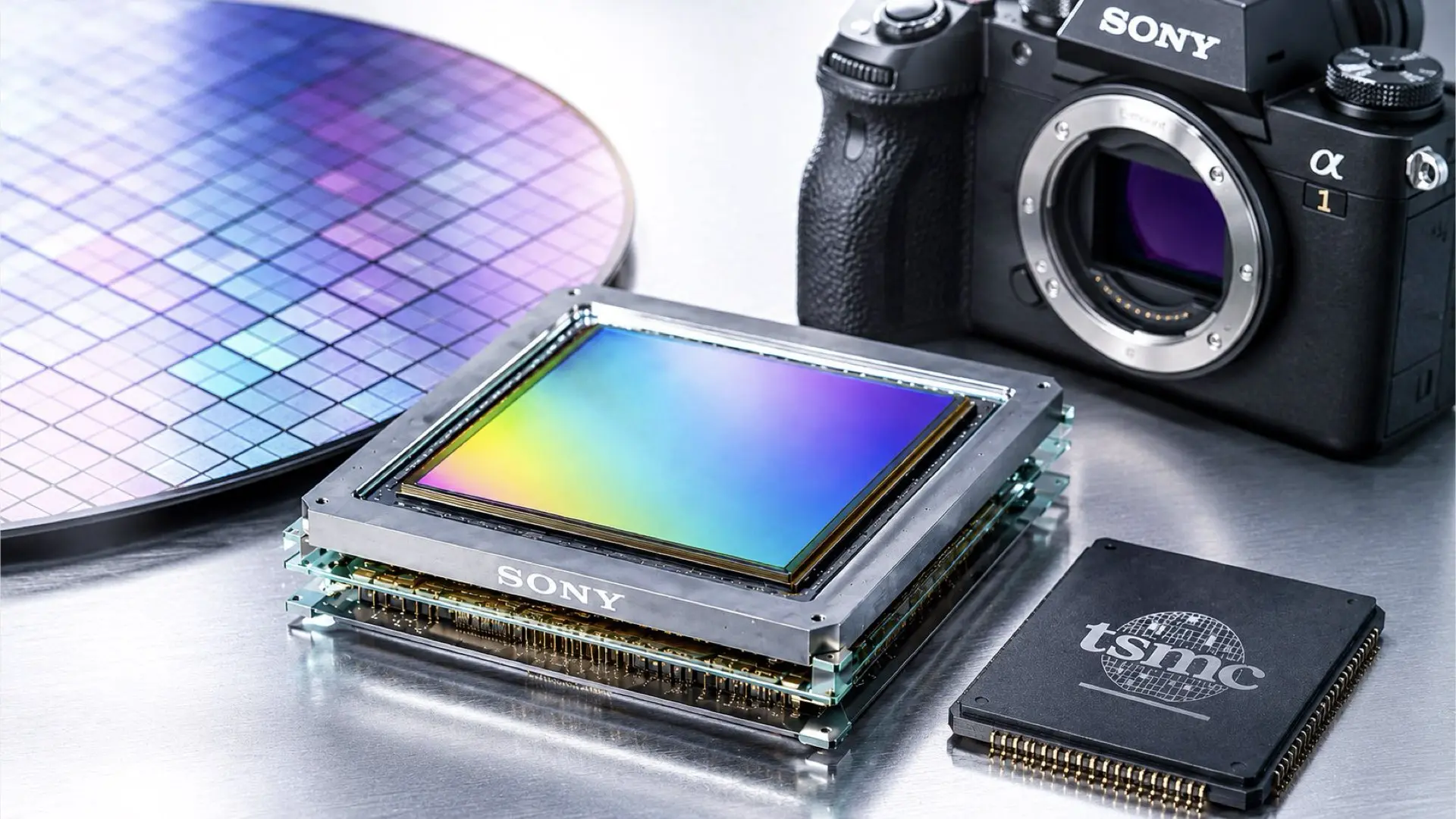
Sony Semiconductor Solutions and TSMC have signed a preliminary agreement to form a strategic partnership for the development and manufacturing of next-generation image sensors. The move could mark a major shift in the future of imaging, as Sony aims to combine its sensor design leadership with TSMC’s process technology and manufacturing expertise. The target is clear. Future image sensors will need to serve cameras, smartphones, cars, robots, and AI-driven machines that rely on vision as their primary sensing tool.
TSMC’s manufacturing expertise could help Sony push more advanced stacked sensor designs, faster readout circuits, improved efficiency, and more sophisticated processing layers. This does not mean that a specific Alpha, FX, VENICE, or smartphone camera is around the corner. The agreement is still preliminary. However, it signals where Sony believes the image sensor industry is heading.
A new joint venture in Japan
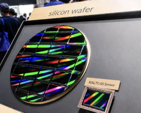
According to the announcement, Sony Semiconductor Solutions and Taiwan Semiconductor Manufacturing Company have signed a non-binding memorandum of understanding to establish a joint venture. Sony is expected to be the majority and controlling shareholder. The JV would set up development and production lines inside Sony’s newly constructed fab in Koshi City, Kumamoto Prefecture, Japan. That detail is important. This is a Sony-led image sensor initiative, with TSMC joining as a strategic manufacturing and process technology partner. Sony remains in control of the sensor business direction, while TSMC contributes the semiconductor manufacturing capabilities that are becoming increasingly critical for advanced sensing architectures. The companies are also discussing potential investments by the JV, along with additional capital investment by Sony in its existing plant in Nagasaki. These investments are expected to be implemented in phases, based on market demand and Japanese government support.
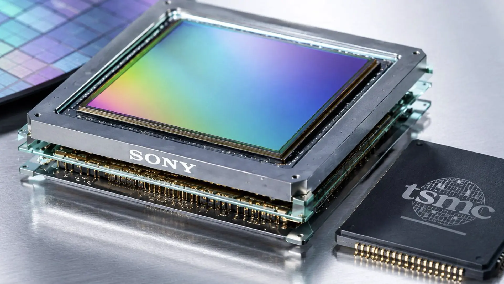
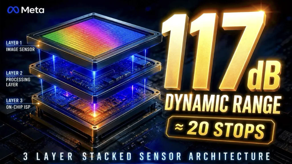
Image sensors are becoming semiconductor platforms
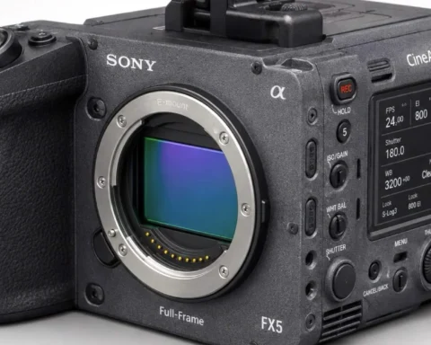
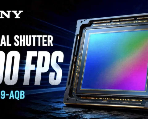
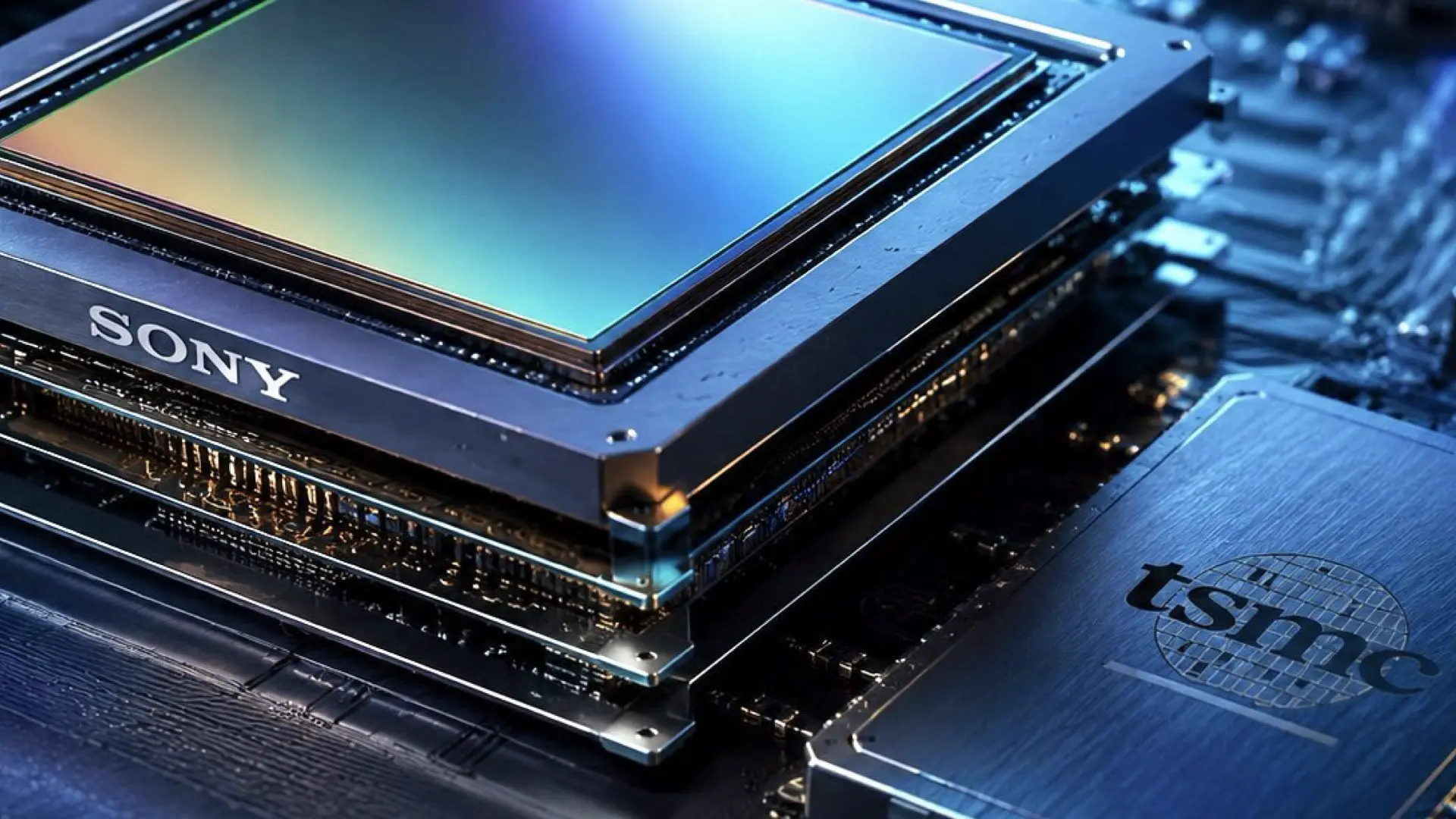
For decades, image sensor progress was mostly discussed through familiar terms such as resolution, pixel size, low light performance, dynamic range, readout speed, and rolling shutter reduction. Those metrics are still essential, especially for filmmakers and camera manufacturers. However, the next stage of sensor development is becoming far more complex. Modern image sensors are no longer simple light-gathering components. They are layered semiconductor platforms. They combine photodiodes, stacked logic, memory, signal processing, AI-related computation, and increasingly specialized readout structures. That is where TSMC becomes highly relevant. TSMC’s manufacturing expertise could help Sony push more advanced stacked sensor designs, faster readout circuits, improved efficiency, and more sophisticated processing layers. This does not mean that a specific Alpha, FX, VENICE, or smartphone camera is around the corner. The agreement is still preliminary. However, it signals where Sony believes the image sensor industry is heading.
What it means for cameras
The first wave of benefits may target smartphones, automotive systems, robotics, and industrial vision. These markets demand huge volumes and fast technology cycles. Cinema cameras and mirrorless cameras usually receive these technologies later, after they mature and become commercially viable. Still, the camera industry should pay attention. Many major camera features started in adjacent markets before reaching professional imaging. Stacked sensors, backside illumination, phase detection pixels, ultra-fast readout, and advanced subject recognition all reflect this broader convergence between consumer imaging, machine vision, and computational photography. For filmmakers, the long-term implications might be significant. More advanced sensor manufacturing could lead to faster readout, better global shutter performance, cleaner high ISO capture, wider dynamic range, and more intelligent image processing pipelines. It could also accelerate the development of sensors optimized for AI-assisted autofocus, subject tracking, exposure control, stabilization, and computational video. In other words, this partnership may begin in the world of physical AI, automotive, and robotics, yet its impact could eventually reach the professional camera space.
More advanced sensor manufacturing could lead to faster readout, better global shutter performance, cleaner high ISO capture, wider dynamic range, and more intelligent image processing pipelines. It could also accelerate the development of sensors optimized for AI-assisted autofocus, subject tracking, exposure control, stabilization, and computational video.
Final thoughts
Sony and TSMC joining forces on next-generation image sensors is a major indication for the imaging industry. The future of sensors will be shaped by stacked architectures, advanced manufacturing, AI-driven perception, automotive vision, robotics, and computational imaging. For our readers, the key takeaway is simple. The image sensor is becoming the brain of the camera system. It is where optics, silicon, processing, and machine intelligence begin to converge. Sony and TSMC are now preparing to build that awesomeness together.